
Shop fromIndia’s Most Affordable Electronics Store
from Rs.99.00
Don't miss this special opportunity today.


Showing 193–208 of 211 resultsSorted by latest

The CD40106 device consists of six Schmitt-Trigger inputs. Each circuit functions as an inverter with Schmitt-Trigger input. The trigger switches at different points for positive- and negative-going signals. The difference between the positive-going voltage (VP) and the negative-going voltages (VN) is defined as hysteresis voltage (VH).
The CD40106 device is supplied in ceramic packaging (J) as well as standard packaging (D, N, NS, PW). All CD40106 devices are rated for –55°C to +125°C ambient temperature operation.

CD4010 Hex Buffer/Converters may be used as CMOS to TTL or DTL logic-level converters or CMOS high-sink-current drivers.
The CD4010 types are supplied in 16-lead hermetic dual-in-line ceramic packages (F3A suffix), 16-lead dual-in-line plastic packages (E suffix)

CD4009 Hex Buffer/Converters may be used as CMOS to TTL or DTL logic-level converters or CMOS high-sink-current drivers.
The CD4009 types are supplied in 16-lead hermetic dual-in-line ceramic packages (F3A suffix), 16-lead dual-in-line plastic packages (E suffix).

CD4008 types consist of four full adder stages with fast look ahead carry provision from stage to stage. Circuitry is included to provide a fast “parallel-carry-out” but to permit high-speed operation in arithmetic sections using several CD4008's. CD4008 inputs include the four sets of bits to be added, A1 to A4 and B1 to B4, in addition to the “Carry In” bit from a previous section. CD4008 outputs include the four sum bits, S1 to S4. In addition to the high speed “parallel-carryout” which may be utilized at a succeeding CD4008 section.

CD4007 IC is comprised of three n-channel and three p-channel enhancement-type MOS transistors. The transistor elements are accessible through the package terminals to provide a convenient means for constructing the various typical circuits.
More complex functions are possible using multiple packages. Numbers shown in parentheses indicate terminals that are connected together to form the various configurations listed.
The CD4007 types are supplied in 14-lead hermetic dual-in-line ceramic packages (F3A suffix), 14-lead dual-in-line plastic packages (E suffix), 14-lead small-outline packages (M, MT, M96, and NSR suffixes), and 14-lead thin shrink small-outline packages (PW and PWR suffixes).

CD4001 NOR gates provide the system designer with direct implementation of the NOR function and supplement the existing family of CMOS gates. All inputs and outputs are buffered.
The CD4001 types are supplied in 14-lead hermetic dual-in-line ceramic packages (F3A suffix).

Arduino UNO uses ATMEGA328P-PU microcontroller and this controller comes pre-loaded with a Arduino UNO bootloader. Basically bootloader is a little piece of code that allows you to program the flash memory of the Arduino’s atmega328p via serial or USB instead of using an ICSP programmer.
If you are making a project based on Arduino UNO & you have made a customized PCB then you will be requiring bootloaded Atmega328 microcontroller. This is a ATmega328 in DIP package, pre-loaded with the Arduino (16MHz) Bootloader. This will allow you to use Arduino code in your custom embedded project without having to use an actual Arduino board. To get this chip working with Arduino IDE, you will need an external 16MHz crystal or resonator, a 5V supply, and a serial connection. You should select the Arduino UNO board within the Arduino IDE.

The P89V51RD2 is an 80C51 microcontroller by NXP (Phillips) with 64 kB Flash and 1024 bytes of data RAM. A key feature of the P89V51RD2 is its X2 mode option. The design engineer can choose to run the application with the conventional 80C51 clock rate (12 clocks per machine cycle) or select the X2 mode (6 clocks per machine cycle) to achieve twice the throughput at the same clock frequency. Another way to benefit from this feature is to keep the same performance by reducing the clock frequency by half, thus dramatically reducing the EMI.
The Flash program memory supports both parallel programming and in serial In-System Programming (ISP). Parallel programming mode offers gang-programming at high speed, reducing programming costs and time to market. ISP allows a device to be reprogrammed in the end product under software control. The capability to field/update the application firmware makes a wide range of applications possible.
The P89V51RD2 is also In-Application Programmable (IAP), allowing the Flash program memory to be reconfigured even while the application is running.

The 80C51 has separate address spaces for program and data memory. The Program memory can be up to 64k bytes long. The lower 4k can reside on-chip. Figure 1 shows a map of the 80C51 program memory. The 80C51 can address up to 64k bytes of data memory to the chip. The MOVX instruction is used to access the external data memory. The 80C51 has 128 bytes of on-chip RAM, plus a number of special function Registers (SFRs). The lower 128 bytes of RAM can be accessed either by direct addressing (MOV data addr) or by indirect addressing (MOV @Ri).

W78E052DDG is a successive microcontroller unit that is fully compatible with the widely popular 8052 despite having an 8051 core. It is an 8-bit architecture-based microcontroller unit that has 8 kilobytes of Flash.
It has 256 bytes of RAM, 4 8-bit bi-directional I/O ports, specified as P0, P1, P2, P3, and 4-bit I/O port P4. Three 16-bit timer/counters, a hardware watchdog timer, and a serial port make this microcontroller easy to integrate with multiple applications.
The specialty of this microcontroller unit is the optional 12T or 6T mode. In 12T mode, it uses 12 clocks per machine cycle where the speed of the processor goes up to 40 MHz at 5V operating voltage. At the same time, if 6T Mode is selected, 6 clocks per machine cycle operation make the controller speed up to 20 MHz at 5V operating voltage.
It supports 2.4V to 5.5V operation, which makes it suitable for 3.3V to 5V logic level operations.

The AT89S8253 is a 8-bit low-power high-performance CMOS Microcontroller with 12kB of In-System Programmable (ISP) flash program memory and 2kB of EEPROM data memory. The device is manufactured using Atmel's high-density non-volatile memory technology and is compatible with the industry-standard MCS-51 instruction set and pinout. The on-chip downloadable flash allows the program memory to be reprogrammed in-system through an SPI serial interface or by a conventional non-volatile memory programmer. By combining a versatile 8-bit CPU with downloadable flash on a monolithic chip, the Atmel AT89S8253 is a powerful microcontroller which provides a highly-flexible and cost-effective solution to many embedded control applications.
The AT89S8252 is a low-power, high-performance CMOS 8-bit microcomputer with 8K bytes of downloadable Flash programmable and erasable read only memory and 2K bytes of EEPROM. The device is manufactured using Atmel’s high-density nonvolatile memory technology and is compatible with the industry-standard 80C51 instruction set and pinout. The on-chip downloadable Flash allows the program memory to be reprogrammed in-system through an SPI serial interface or by a conventional nonvolatile memory programmer. By combining a versatile 8-bit CPU with downloadable Flash on a monolithic chip, the Atmel AT89S8252 is a powerful microcomputer which provides a highly-flexible and cost-effective solution to many embedded control applications.

The Atmel AT89S52 Microcontroller or commonly known as AT89S52 is a low-power, high-performance CMOS 8-bit microcontroller with 8K bytes of in-system programmable Flash memory. The device is manufactured using Atmel’s high-density nonvolatile memory technology and is compatible with the industry-standard 80C51 instruction set and pinout. The on-chip Flash allows the program memory to be reprogrammed in-system or by a conventional nonvolatile memory programmer. By combining a versatile 8-bit CPU with in-system programmable Flash on a monolithic chip, the Atmel AT89S52 is a powerful microcontroller which provides a highly-flexible and cost-effective solution to many embedded control applications.

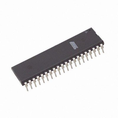
AT89S51 Microcontroller

The AT89C55 is a 8-bit low-power High-performance CMOS Microcontroller with 20kB of flash programmable read only memory and 256 bytes of RAM. The device is manufactured using Atmel's high-density non-volatile memory technology and is compatible with the industry standard 80C51 and 80C52 instruction set and pinout. The on-chip Flash allows the program memory to be user programmed by a conventional non-volatile memory programmer. By combining a versatile 8-bit CPU with flash on a monolithic chip, the Atmel AT89C55 is a powerful microcomputer which provides a highly flexible and cost effective solution to many embedded control applications. The AT89C55 provides the following standard features 20kB of Flash, 256 bytes of RAM, 32 I/O lines, three 16-bit timer/counters, a six-vector, two-level interrupt architecture, a full-duplex serial port, on-chip oscillator and clock circuitry.

The AT89C52 is a low-power, high-performance CMOS 8-bit microcomputer with 8K bytes of Flash programmable and erasable read only memory (PEROM). The device is manufactured using Atmel’s high density nonvolatile memory technology and is compatible with the industry standard 80C51 and 80C52 instruction set and pin out. The on-chip Flash allows the program memory to be reprogrammed in-system or by a Conventional nonvolatile memory programmer. By combining a versatile 8-bit CPU With Flash on a monolithic chip, the Atmel AT89C52 is a powerful microcomputer which provides a highly flexible and cost effective solution to many embedded control applications.