
Shop fromIndia’s Most Affordable Electronics Store
from Rs.99.00
Don't miss this special opportunity today.


Showing 209–224 of 262 resultsSorted by latest
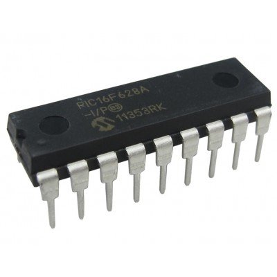
The PIC16F628A is 18-pin Flash-based members of the versatile PIC16F628A family of low-cost, high-performance, CMOS, fullystatic, 8-bit microcontrollers. All PIC® microcontrollers employ an advanced RISC architecture. The PIC16F628A have enhanced core features, an eight-level deep stack, and multiple internal and external interrupt sources. The separate instruction and data buses of the Harvard architecture allow a 14-bit wide instruction word with the separate 8-bit wide data. The two-stage instruction pipeline allows all instructions to execute in a single cycle, except for program branches (which require two cycles). A total of 35 instructions (reduced instruction set) are available, complemented by a large register set.
PIC16F628A microcontrollers typically achieve a 2:1 code compression and a 4:1 speed improvement over other 8-bit microcontrollers in their class. PIC16F628A devices have integrated features to reduce external components, thus reducing system cost, enhancing system reliability and reducing power consumption.

CD40193 up/down counters are monolithic complementary MOS (CMOS) integrated circuits. The CD40192BM and CD40192BC are BCD counters, while the CD40193BM and CD40193BC are binary counters.
Counting up and counting down is performed by two count inputs, one being held high while the other is clocked. The outputs change on the positive-going transition of this clock.
These counters feature preset inputs that are enabled when load is a logical ‘‘0’’ and a clear which forces all outputs to ‘‘0’’ when it is at logical ‘‘1’’. The counters also have carry and borrow outputs so that they can be cascaded using no external circuitry. All inputs are protected against damage due to static discharge by clamps to VDD and VSS.

PIC16F616 Microcontroller
The PIC16F range of microcontrollers from Microchip are 8-bit MCUs that incorporate Microchip’s PIC® architecture into a variety of pin and package options, from space efficient 14-pin devices to feature-rich 64-pin devices. Devices with Baseline, Mid-Range or Enhanced Mid-Range architecture are available with numerous different peripheral combinations, giving designers flexibility and choice for their applications.
The PIC16F616 family of microcontrollers is based upon Microchip’s Mid-Range core with a 8 level deep hardware stack and 35 instructions. These MCUs provide up to 5 MIPS, up to 3.5 Kbytes program memory, up to 128 bytes RAM and Data EEPROM of up to 128 bytes. On board is a configurable oscillator factory calibrated to ±1% accuracy.

The CD4017 is a 5-stage divide-by-10 Johnson counter with 10 decoded outputs and a carry out bit. The configuration of the CD4017 permits medium speed operation and assures a hazard free counting sequence. The 10/8 decoded outputs are normally in the logical “0” state and go to the logical “1” state only at their respective time slot. Each decoded output remains high for 1 full clock cycle. The carry-out signal completes a full cycle for every 10/8 clock input cycles and is used as a ripple carry signal to any succeeding stages.

The CD4016 is a quad bilateral switch intended for the transmission or multiplexing of analog or digital signals. It is pin-for-pin compatible with CD4066B.

The PIC16F505 devices from Microchip Technology are low-cost, high-performance, 8-bit, fully-static, Flash-based CMOS microcontrollers. They employ a RISC architecture with only 33 single-word/ single-cycle instructions. All instructions are single cycle (200 μs) except for program branches, which take two cycles. The PIC16F505 devices deliver performance an order of magnitude higher than their competitors in the same price category. The 12-bit wide instructions are highly symmetrical, resulting in a typical 2:1 code compression over other 8-bit microcontrollers in its class. The easy to use and easy to remember instruction set reduces development time significantly.
The PIC16F505 products are equipped with special features that reduce system cost and power requirements. The Power-on Reset (POR) and Device Reset Timer (DRT) eliminate the need for external Reset circuitry. There are four oscillator configurations to choose from (six on the PIC16F505), including INTRC Internal Oscillator mode and the power-saving LP (Low-Power) Oscillator mode. Power-Saving Sleep mode, Watchdog Timer and code protection features improve system cost, power and reliability.
The PIC16F505 devices are available in the cost-effective Flash programmable version, which is suitable for production in any volume. The customer can take full advantage of Microchip’s price leadership in Flash programmable microcontrollers, while benefiting from the Flash programmable flexibility.

CD4015 consists of two identical, independent, 4-stage serial-input/parallel-output registers. Each register has independent CLOCK and RESET inputs as well as a single serial DATA input. "Q" outputs are available from each of the four stages on both registers. All register stages are D-type, master-slave flip-flops. The logic level present at the DATA input is transferred into the first register stage and shifted over one stage at each positive-going clock transition. Resetting of all stages is accomplished by a high level on the reset line. Register expansion to 8 stages using one CD4015 package, or to more than 8 stages using additional CD4015’s is possible.
The CD4015-series types are supplied in 16-lead hermetic dual-in-line ceramic packages (F3A suffix), 16-lead dual-in-line plastic package (E suffix), 16-lead small-outline packages (M, M96, MT, and NSR suffixes), and 16-lead thin shrink small-outline packages (PW and PWR suffixes).

The CD4013 device consists of two identical, independent data-type flip-flops. Each flip-flop has independent data, set, reset, and clock inputs and Q and Q outputs. These devices can be used for shift register applications, and, by connecting Q output to the data input, for counter and toggle applications. The logic level present at the D input is transferred to the Q output during the positive-going transition of the clock pulse. Setting or resetting is independent of the clock and is accomplished by a high level on the set or reset line, respectively.
The CD4013 types are supplied in 14-pin dual-in-line plastic packages (E suffix), 14-pin small-outline packages (M, MT, M96, and NSR suffixes), and 14-pin thin shrink small-outline packages (PW and PWR suffixes).

The PIC16F1503-I/P is an enhanced mid-range PIC16 family 8-bit powerful (200 nanosecond instruction execution) yet easy-to-program CMOS flash-based Microcontroller packs powerful PIC®(RISC) architecture. This product offers all of the advantages of the well-recognized mid-range x14 architecture with standardized features including 3.5kB of addressable program memory size, 128bytes of data memory size, 12 general-purpose I/O pins, two comparators, 8-channel 10-bit analog-to-digital (A/D) converter, and one 5-bit digital-to-analog (D/A) converter. This device operates at a maximum frequency of 20MHz with a wide operating voltage of 1.8 to 5.5V.
- 49 (14-bit wide) easy instructions to learn
- Hardware interrupt handling with the content save
- Programmable brown-out reset (BOR)
- Power-on reset (POR)
- Internal voltage reference (Bandgap)
- Four stand-alone PWM
- 2x Configurable logic cell modules (CLC)
- 1x Complementary waveform generator (CWG)/Complementary output generator (COG)
- Numerically controlled oscillator (NCO)
- In-Circuit Serial Programming (ICSP)

The NAND gate is monolithic complementary MOS (CMOS) integrated circuits. The N- and P-channel enhancement mode transistors provide a symmetrical circuit with output swings essentially equal to the supply voltage. This results in high noise immunity over a wide supply voltage range. No DC power other than that caused by leakage current is consumed during static conditions. All inputs are protected against static discharge and latching conditions.

CD4011 NAND gates provide the system designer with direct implementation of the NAND function and supplement the existing family of CMOS gates. All inputs and outputs are buffered.
The CD4011 type are supplied in 14-lead hermetic dual-in-line ceramic packages (F3A suffix), 14-lead dual-in-line plastic packages (E suffix), 14-lead small-outline packages (M, MT, M96, and NSR suffixes), and 14-lead thin shrink small-outline packages (PWR suffix). The CD4011 type also are supplied in 14-lead thin shrink small-outline packages (PW suffix).

The PIC16C711 is a low-cost, high-performance, CMOS, fully-static, 8-bit microcontrollers with integrated analog-to-digital (A/D) converters, in the PIC16C711 mid-range family. The separate instruction and data buses of the Harvard architecture allow a 14-bit wide instruction word with the separate 8-bit wide data. The two stage instruction pipeline allows all instructions to execute in a single cycle, except for program branches which require two cycles. A total of 35 instructions (reduced instruction set) are available. Additionally, a large register set gives some of the architectural innovations used to achieve a very high performance. PIC16C711 microcontrollers typically achieve a 2:1 code compression and a 4:1 speed improvement over other 8-bit microcontrollers in their class. The PIC16C711 devices have 36 bytes of RAM, the PIC16C711 has 68 bytes of RAM and the PIC16C715 has 128 bytes of RAM. Each device has 13 I/O pins. In addition a timer/counter is available. Also a 4-channel high-speed 8-bit A/D is provided.

CD40109 contains four low-to-high-voltage level-shifting circuits. Each circuit will shift a low-voltage digital-logic input signal (A, B, C, D) with logical 1 = VCC and logical 0 = VSS to a high-voltage output signal (E, F, G, H) with logical 1 = VDD and logical 0 = VSS.
The RCA-CD40109, unlike other low-to-high level-shifting circuits, does not require the presence of the high-voltage supply (VDD) before the application of either the low-voltage supply (VCC) or the input signals. There are no restrictions on the sequence of application of VDD, VCC, or the input signals. In addition, with one exception there are no restrictions on the relative magnitudes of the supply voltages or input signals within the device maximum ratings, provided that the input signal swings between VSS and at least 0.7 VCC; VCC may exceed VDD, and input signals may exceed VCC and VDD. When operated in the mode VCC > VDD, the CD40109 will operate as a high-to-low level-shifter.
The CD40109 also features individual three-state output capability. A low level on any of the separately enabled three-state output controls produces a high-impedance state in the corresponding output.

The PIC16C63A devices are low cost, high performance, CMOS, fully-static, 8-bit microcontrollers in the PIC16CXX mid-range family. All PIC® microcontrollers employ an advanced RISC architecture. The PIC16CXX microcontroller family has enhanced core features, eight-level deep stack and multiple internal and external interrupt sources. The separate instruction and data buses of the Harvard architecture allow a 14-bit wide instruction word with the separate 8-bit wide data. The two stage instruction pipeline allows all instructions to execute in a single cycle, except for program branches, which require two cycles. A total of 35 instructions (reduced instruction set) are available. Additionally, a large register set gives some of the architectural innovations used to achieve a very high performance. The PIC16C63 devices have 22 I/O pins. Each device has 192 bytes of RAM. In addition, several peripheral features are available, including: three timer/ counters, two Capture/Compare/PWM modules, and two serial ports. The Synchronous Serial Port (SSP) can be configured as either a 3-wire Serial Peripheral Interface (SPI) or the two-wire Inter-Integrated Circuit (I2C) bus.

The CD40106 device consists of six Schmitt-Trigger inputs. Each circuit functions as an inverter with Schmitt-Trigger input. The trigger switches at different points for positive- and negative-going signals. The difference between the positive-going voltage (VP) and the negative-going voltages (VN) is defined as hysteresis voltage (VH).
The CD40106 device is supplied in ceramic packaging (J) as well as standard packaging (D, N, NS, PW). All CD40106 devices are rated for –55°C to +125°C ambient temperature operation.

The PIC16C622 device has enhanced core features, eight-level deep stack, and multiple internal and external interrupt sources. The separate instruction and data buses of the Harvard architecture allow a 14-bit wide instruction word with the separate 8-bit wide data. The two-stage instruction pipeline allows all instructions to execute in a single cycle, except for program branches (which require two cycles). A total of 35 instructions (reduced instruction set) are available. Additionally, a large register set gives some of the architectural innovations used to achieve a very high performance. PIC16C622 micro controllers typically achieve a 2:1 code compression and a 4:1 speed improvement over other 8-bit micro controllers in their class.